PBGA package substrate (Computers - Hardware)

Item ID 2997469 in Category: Computers - Hardware
PBGA package substrate | |
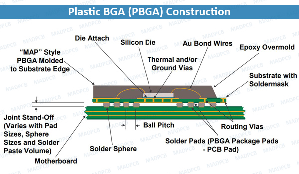
BGA or ball grid array substrates are widely used in the packaging of ICs, ASICs, GPUs, and other multifaceted parts. By allowing a high number of contacts in a limited space it facilitates miniaturization and performance improvements across most forms of electronics. It is important to note, however, that the design of products using and the manufacturing of PBGA package substrate involves fairly complex knowledge. Contact Info:- High Quality PCB Co., Limited Office: Shajing Town, Baoan District, Shenzhen, Guangdong 518000, China Plant 1 address: Building 5-6, Fu Qiao 3rd Industrial Zone, Bao' an, Shenzhen, Guangdong, China Plant 2 address: Zhuhai, Guangdong, China Plant 3 address: Dongguan, Guangdong, China TEL: +86-755-23724206 WahtsApp: +86-189 2381 2997 Skype: shawnwang2006 Email: sales@efpcb.com  | |
| Target State: All States Target City : Shenzhen Last Update : 30 September 2024 4:58 PM Number of Views: 74 | Item Owner : Shawn Wang Contact Email: Contact Phone: +86-755-23724206 |
| Friendly reminder: Click here to read some tips. | |
© 2025 INNetAds.com
USNetAds.com | GetJob.us | CANetAds.com | UKAdsList.com | AUNetAds.com | CNNetAds.com | Hot-Web-Ads.com | USAOnlineClassifieds.com
2025-04-12 (0.455 sec)